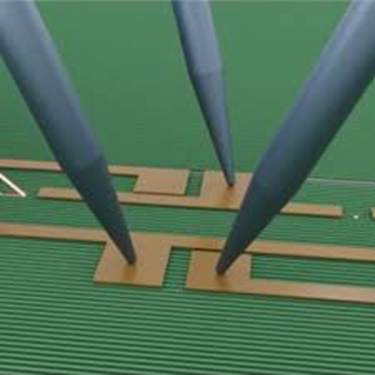
Scientists have successfully integrated lasers directly onto silicon wafers, marking a breakthrough in silicon photonics. This innovation promises faster, more energy-efficient data transmission and could revolutionize computing, particularly in data centers and quantum computing.
Relevance : GS 3(Science and Technology)
Revolutionizing Computing with Silicon Photonics:
- Silicon photonics involves replacing electrons with photons (particles of light) for storing and manipulating information, which has the potential to enhance computing efficiency.
- Laser integration on silicon chips marks a significant breakthrough, allowing lasers to be grown directly onto silicon, eliminating the need for separate laser light sources.
- This integration can make photonic chips scalable, more efficient, and easier to produce compared to previous methods.
Background on Silicon Photonics:
- Silicon chips, a cornerstone of modern communication technologies, have traditionally used electrons to carry information.
- Researchers are now exploring silicon photonics to carry information via photons, as they move faster, offer greater data capacity, and experience fewer energy losses than electrons.
- While photons are promising, integrating a light source (laser) directly onto the silicon chip was a major challenge.
Challenges in Integrating Lasers with Silicon:
- Silicon’s inefficiency in emitting light: Silicon has an indirect bandgap, meaning electrons cannot emit photons efficiently without external energy sources, unlike direct bandgap materials such as gallium arsenide (GaAs).
- The mismatch between silicon and gallium arsenide (used for efficient light emission) led to defects, which hindered light emission and reduced efficiency.
Key Innovations in the Study:
- Researchers successfully fabricated miniaturized lasers directly onto a silicon wafer, solving the integration problem by using a nanostructured design with gallium arsenide.
- Nanometer-wide ridges were carved into a 300-mm silicon wafer, with silicon dioxide serving as an insulating material. This confined defects to the trench’s bottom, allowing for defect-free gallium arsenide growth above.
- Indium gallium arsenide layers were deposited, replacing some gallium atoms with indium to optimize light emission, forming the laser.
Efficient Laser Fabrication:
- The team successfully embedded 300 functional lasers on a single 300-mm silicon wafer, the industry standard for semiconductor manufacturing, ensuring compatibility with existing infrastructure.
- The laser emitted light with a wavelength of 1,020 nm, suitable for short-range transmissions between computer chips.
- The laser operates with a low threshold current (5 mA), similar to that of an LED in a computer mouse, making it energy-efficient.
Promising Results and Future Prospects:
- Energy efficiency: The laser’s output reached around 1MW, and it could run continuously for 500 hours at room temperature (25°C), although efficiency drops at higher temperatures (55°C).
- Challenges in temperature stability: While the laser is efficient at lower temperatures, research has demonstrated continuous operation at higher temperatures (up to 120°C) for optical silicon chips, highlighting areas for further improvement.
- Scalability and cost-effectiveness: The monolithic fabrication process is scalable, meaning more lasers can be integrated on larger wafers at a relatively low cost, offering a potential breakthrough in chip manufacturing.
Impact on Computing:
- The integration of lasers directly onto silicon chips could lead to faster and more energy-efficient data transmission within data centers, where speed and energy consumption are critical factors.
- This new photonic silicon chip technology could significantly boost computing performance, making it viable for quantum computing and other high-demand applications.
Conclusion:
- The demonstration of monolithic laser diodes on silicon wafers represents a major milestone in the evolution of silicon photonics, opening the door to next-generation computing technologies.
- With the process being cost-effective and scalable, this innovation is poised to transform industries by enhancing performance and reducing the energy footprint of future computing systems.